Under the Hood: STM32 Bus Matrix, Memory Map, and the Unaligned Access Secret

Introduction: The Smart Factory Metaphor
Welcome to the theoretical deep dive! Today, we will visualize the “brain map” of the STM32. As a technical writer, I aim to transform complex architectural concepts into a layout as clear as a city blueprint.
Level: ⭐⭐⭐ Intermediate/Advanced Read Time: ~15 Minutes
Imagine the STM32F4 is a massive “Smart Factory”:
- Cortex-M4 Core: The “Factory Manager” (CPU) who issues orders.
- Flash Memory: The “Reference Library” storing the instruction manual (Code).
- SRAM: The “Workbench” holding current documents and projects (Variables).
- Peripherals (GPIO, UART): The “Shipping & Receiving Dept” interfacing with the outside world.
- Bus Matrix: The “Roads and Highways” connecting everything.
Understanding these “roads” (Bus) and the “map” (Memory Map) is the key to writing high-performance code and debugging elusive Hard Faults.
2. The Bus Matrix: Multi-Lane Highways
A common misconception is that the CPU accesses RAM and Peripherals via a single road (Bottleneck). However, the STM32F4 (Harvard Architecture) uses a Multi-AHB Bus Matrix.
2.1 The CPU’s Master Ports
The CPU has three main “limbs” or ports to work in parallel:
- I-Bus (Instruction Bus): An express lane strictly for fetching instructions from Flash. It doesn’t carry data.
- D-Bus (Data Bus): Dedicated to transporting data (literals, variables) and debugging information. It connects directly to the CCM (Core Coupled Memory) for zero-wait state access.
- S-Bus (System Bus): The main road connecting to Peripherals and standard SRAM.
2.2 The Traffic Circle (Bus Matrix)
The Bus Matrix acts like a “Smart Roundabout” that allows Masters (CPU, DMA1, DMA2, Ethernet) to talk to Slaves (Flash, RAM, Peripherals) simultaneously.
The Magic Moment: While the CPU is fetching code from Flash (via I-Bus), the DMA can transfer data from UART to RAM (via System Bus) at the same time. No traffic jams. This concurrency is the secret behind STM32F4’s performance.
3. The Memory Map: One Map to Rule Them All
The ARM Cortex standard dictates a single, flat 4GB (32-bit) address space. Everything—RAM, Flash, hardware registers—has a unique “House Number” (Address).
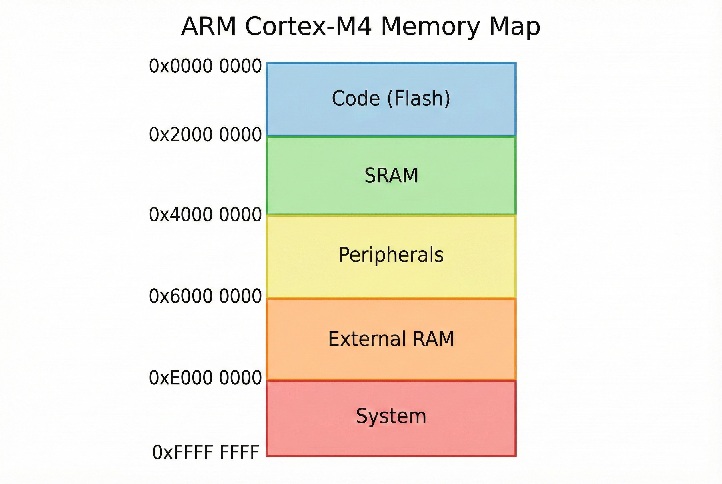
Here is the zoning plan:
| Address Range (Hex) | Region Name | Function |
|---|---|---|
0x0000 0000 |
Code (Boot) | Usually aliased to Flash or Bootloader memory depending on BOOT pin configuration. |
0x0800 0000 |
Flash Memory | The physical location where your program code lives. |
0x2000 0000 |
SRAM | Main working memory (SRAM1, SRAM2) for variables and stack. |
0x4000 0000 |
Peripherals | Home of hardware modules (GPIO, UART, Timers). Split into APB1, APB2, and AHB. |
0xE000 0000 |
System | Restricted CPU area (NVIC, SysTick, Debug components). |
4. Unaligned Access: Convenience vs. Cost
In older architectures (like ARM7 or Cortex-M0), if you declared a 4-byte integer (int), it had to be placed at an address divisible by 4 (0, 4, 8, C). If placed at address 1, the system would crash immediately (Hard Fault).
The Cortex-M3/M4 (STM32F4) is smarter. It supports Unaligned Access.
The Scenario
Imagine a uint32_t val (4 bytes) placed at address 0x20000001 (not divisible by 4).
- Cortex-M0: Triggers a Usage Fault. 💥
- Cortex-M4: Reads the value correctly! The hardware secretly performs two memory reads and stitches the bytes together for you.
The Catch ⚠️
While convenient, this feature comes with a price:
- Performance Penalty: It consumes more bus cycles (2 reads instead of 1).
- Atomicity: Unaligned reads are not atomic. An interrupt could theoretically occur between the first and second partial read.
- Specific Instructions: Some assembly instructions like
LDRD(Load Double) orLDM(Load Multiple) still require alignment. If the compiler generates these instructions for unaligned data, you will still get a Hard Fault.
Best Practice: Always try to keep your data structures aligned (using Structure Padding) for maximum performance. But know that for packed data streams (like from UART), the Cortex-M4 has your back.